
 Hello, I'm Yeting Yang from the Modular Quantum Core Project at the Quantum Laboratory.
In this Tech Blog, I will introduce our recent work on a diamond–Al₂O₃ hybrid structure for scalable quantum photonic chips. The structure integrates Tin-Vacancy (SnV)-containing diamond nanobeams with Al₂O₃ waveguides, enabling efficient optical coupling from diamond emitters to an on-chip optical routing layer. In the following sections, I will discuss the device concept, key fabrication technologies, and our demonstration of guided SnV emission. This work was carried out through collaborations with Delft University of Technology and The University of Tokyo.
1. Overview and Device Concept
Diamond color centers, including Nitrogen-Vacancy (NV) and SnV centers, are promising building blocks for quantum networking and quantum computing because they combine optically accessible transitions with long-lived spin states capable of storing quantum information. Among them, SnV centers are particularly attractive for integrated quantum photonic devices due to their favorable optical characteristics. However, achieving efficient integration of individual diamond emitters into large-scale photonic circuits remains a significant challenge. A practical photonic platform must simultaneously provide high optical coupling efficiency and compatibility with scalable fabrication technologies.
To address these requirements, we developed a hybrid architecture that combines diamond nanobeams containing SnV centers with Al₂O₃ waveguides, leveraging the strengths of both material platforms.
2. Hybrid Optical Structure
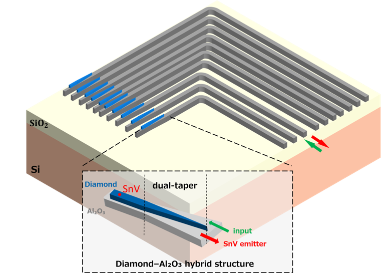
To realize this concept, we designed a diamond–Al₂O₃ dual-taper structure. In this design, the widths of both the diamond nanobeam and the Al₂O₃ waveguide are gradually varied around the interface region, enabling efficient photon transfer between the diamond layer and the underlying waveguide.
The hybrid structure supports bidirectional waveguide-based light excitation and collection of SnV centers. Green excitation light is coupled into the diamond nanobeam through the waveguide, and the resulting emission from the SnV centers is subsequently collected back into the same waveguide.
3. Demonstration of Guided SnV Emission
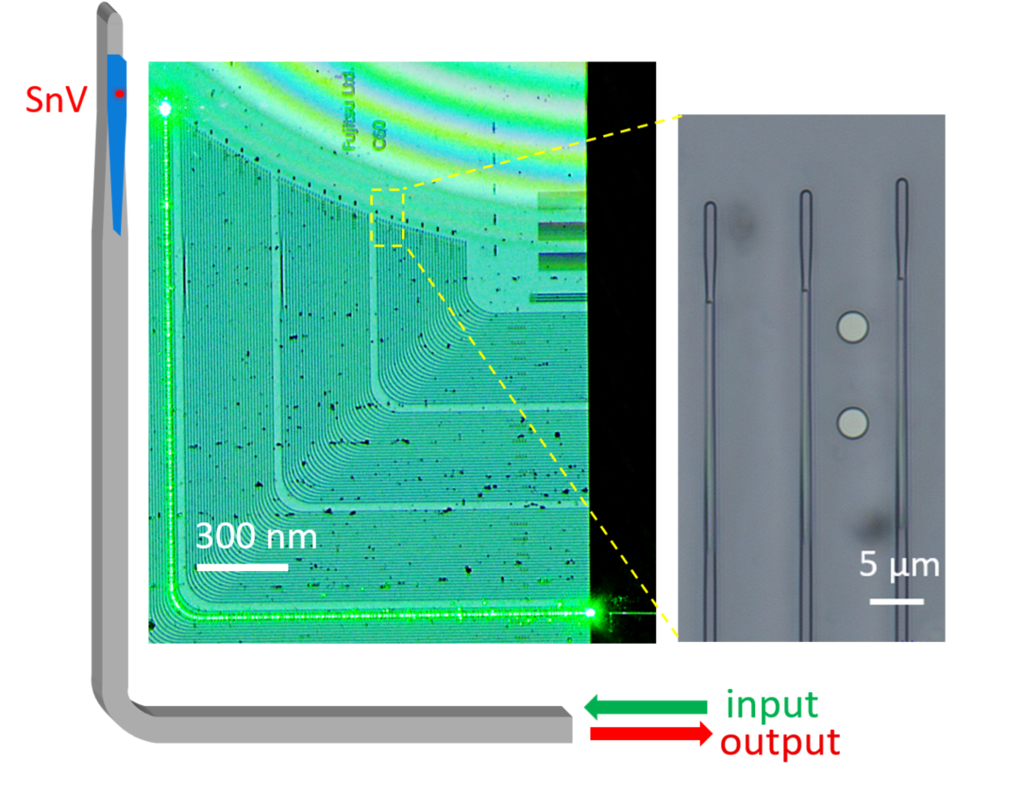
The hybrid devices were fabricated using a bilayer process compatible with scalable lithography. Several fabrication challenges had to be addressed, including thinning bulk diamond from an initial thickness of 500 μm to the sub-micrometer regime, selectively etching diamond while preserving the underlying Al₂O₃, and precisely aligning the diamond nanobeam with the Al₂O₃ waveguide. To address these challenges, we used a multi-step thinning process combining laser slicing, mechanical polishing, and dry etching, while reducing the Inductively Coupled Plasma (ICP) power and bias power during nanobeam etching to protect the Al₂O₃ layer. A uniform electron-beam lithography process with alignment markers was also used for precise alignment. These process technologies are essential for reproducibly integrating diamond quantum emitters with Al₂O₃ photonic circuits. To evaluate device performance, we carried out room-temperature optical measurements of SnV photoluminescence guided through the Al₂O₃ waveguide. The measurements clearly revealed the characteristic SnV zero-phonon line near 620 nm.
Importantly, guided SnV emission was successfully observed in more than 83% of the measured devices, demonstrating the high reproducibility of the fabrication process and the effectiveness of the hybrid structure for coupling emission from embedded SnV centers into integrated photonic waveguides.
4. Future Developments
This work demonstrates a device platform for multi-module integration and optical coupling between SnV-containing diamond nanobeams and Al₂O₃ waveguides. The key enabling technologies are the diamond–Al₂O₃ dual-taper design and the bilayer fabrication process, which facilitate integration of the diamond emitter layer with an Al₂O₃-based optical routing layer.
Moving forward, we aim to further improve optical coupling efficiency and incorporate additional photonic functionalities, including optical switches, wavelength-tuning elements, and routing circuits. These components will be essential for connecting multiple diamond-based quantum nodes and enabling sophisticated on-chip optical control. Looking further ahead, the diamond–Al₂O₃ hybrid integration approach represents a practical pathway toward modular quantum photonic architectures, in which diamond color centers serve as quantum nodes and integrated waveguides provide scalable optical interconnects between them.
For more details, please refer to our paper [1].
[1] Y. Yang et al., Jpn. J. Appl. Phys. 65, 170902 (2026). DOI: 10.35848/1347-4065/ae91b1
